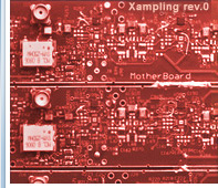
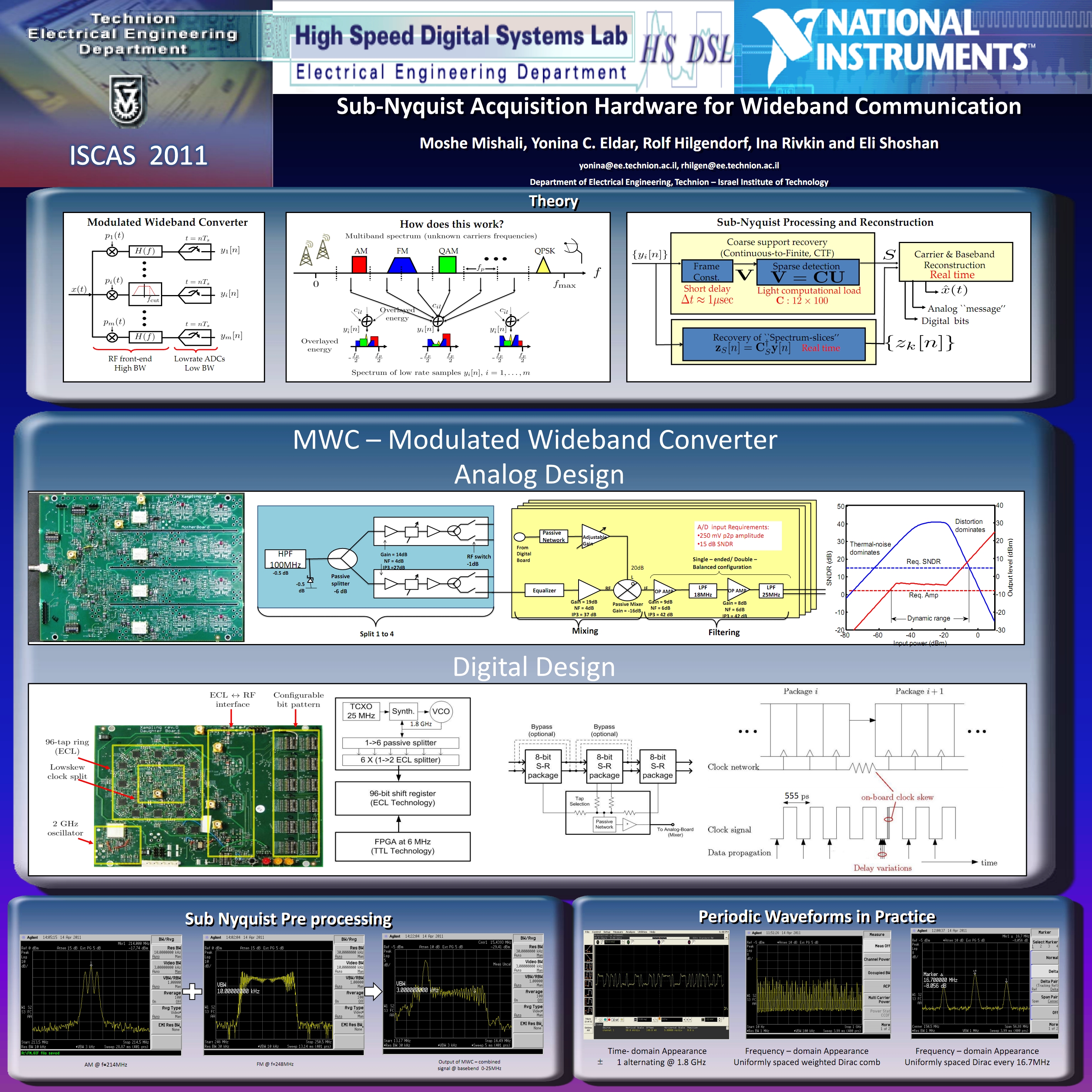
Data Acquisition
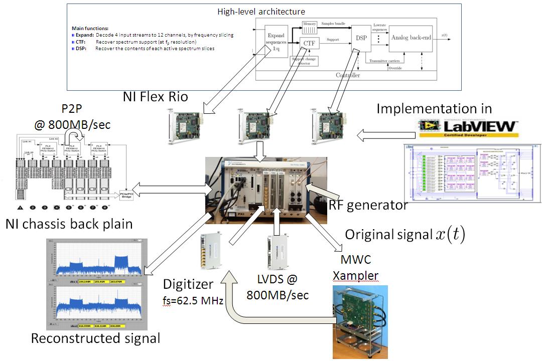
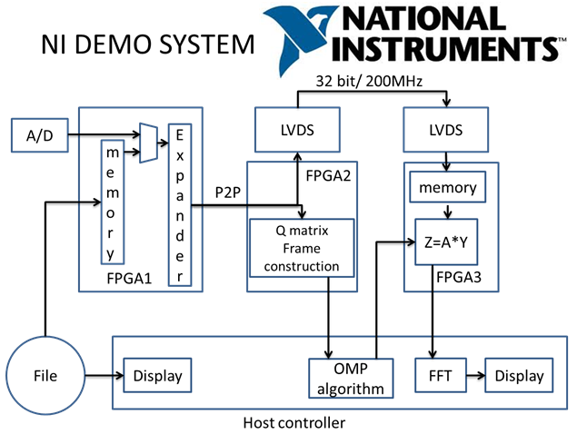
As shown in Figure 3, two signals are produced by NI 5651 RF generators and combined using a Mini Circuit RF combiner. Thereafter the combined signal is entered into the MWC card where it is pre-processed and split into 4 channels as described in the sub-Nyquist signal acquisition page.
The four channels are sampled using the NI 5761 A/D at 62.5 MHz. The samples are saved to a CSV file on the chassis's hard drive.
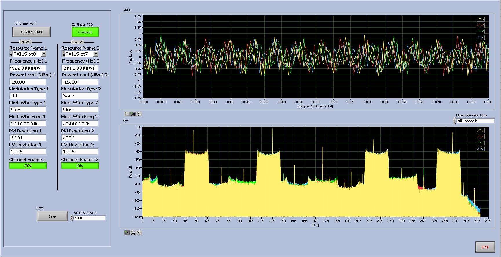
Figure 3 - Data acquisition front panel.
On the left hand side are the controls for each of the two RF generators. At first the carrier frequency is selected as well as the power level of the output signal. The next set of fields deal with the modulation. In Modulation Type we can select None, FM or PM. If any modulation is selected, the next field selects the form of the modulating waveform Sine, Square or Triangle, and the following field selects the frequency of the modulating wave form. The final two fields select the bandwidth (deviation) of the modulated signal. The last button in each of the two sides enables or disables Signal Generation.
Above the control of the RF generators there are two buttons, 'Acquire Data' which starts a single acquisition cycle and 'Continuous Acq' which controls if we do single acquisition or loop through acquisitions indefinitely. At the bottom we have a button which starts saving data onto disc. Next to it is a selector for the number of samples to save. If continuous acquisition is selected, saving data always starts from the beginning of the next loop cycle.
On the right hand side we display the sampled data. On the top we show the time-domain signal, while the bottom shows the power spectrum of the sampled signal. We may select if to display all channels together or displaying them on a channel by channel basis.
Finally in the lower left hand corner is the stop button which stops execution at the end of the current loop cycle.
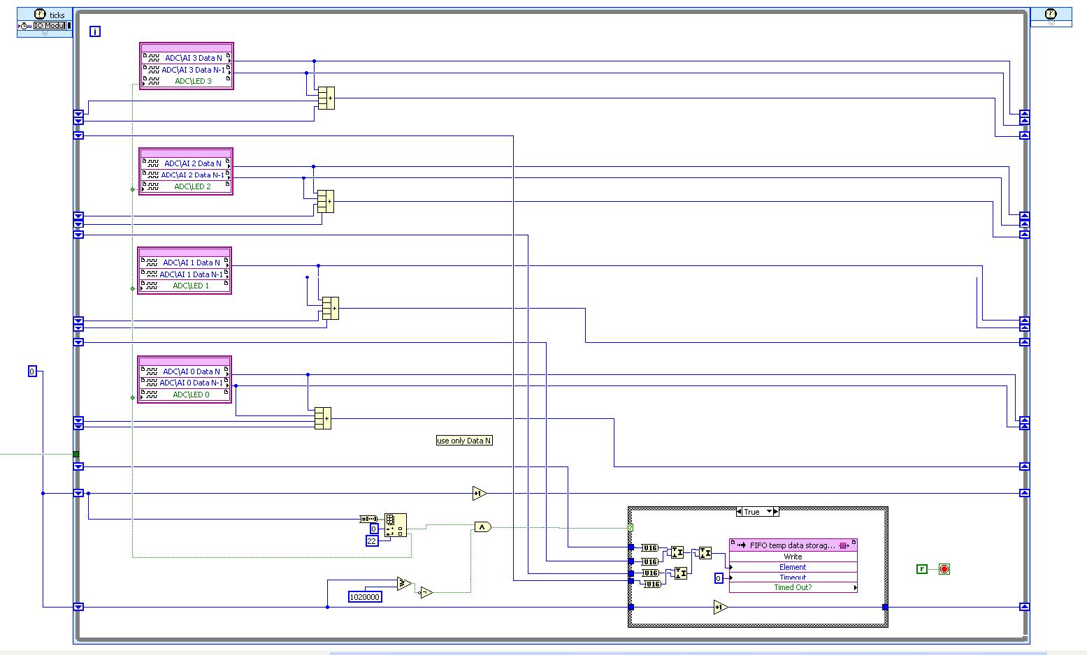
Figure 4 - Acquisition block diagram.
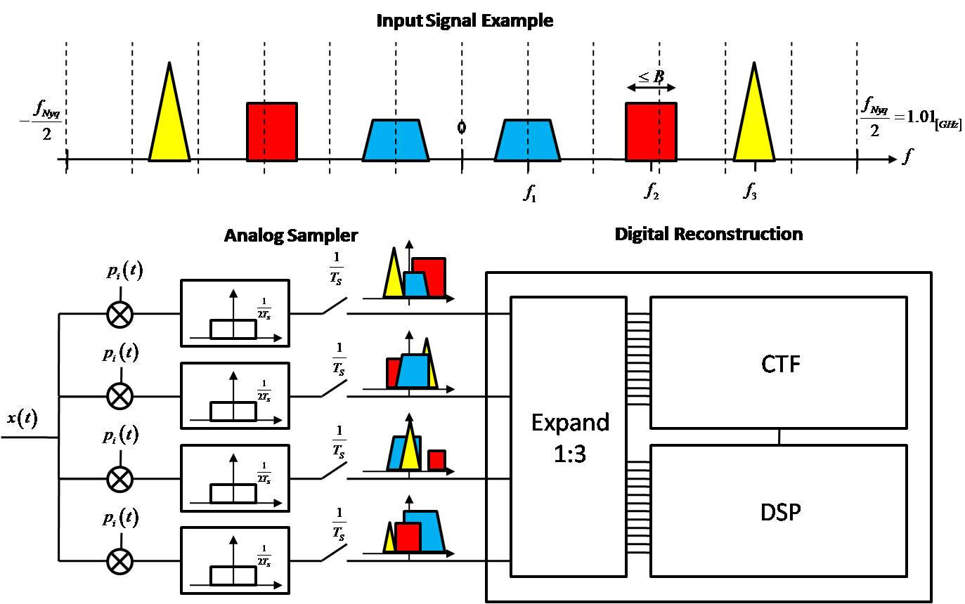
Data Reconstruction
Figure 5 - Block diagram of the data flow in reconstruction.
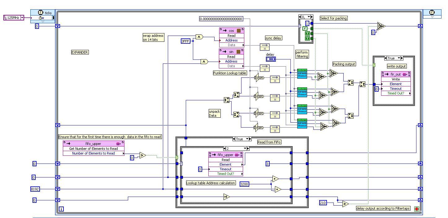
Reconstruction starts with loading the samples from file and sending them to the 1st FPGA, the expander unit. In the expander the samples are filtered using polyphase filters so that each channel is split into 3 slices. These slices are sent to the 2nd FPGA through a p2p connection at 800 MB/sec.
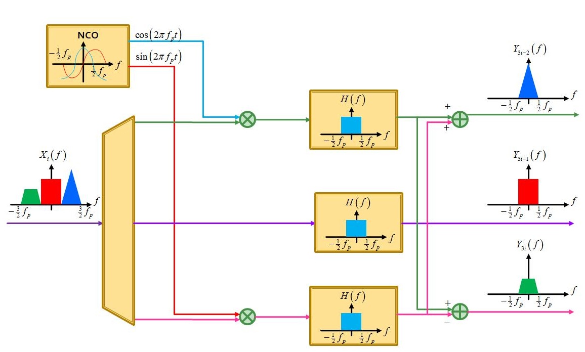
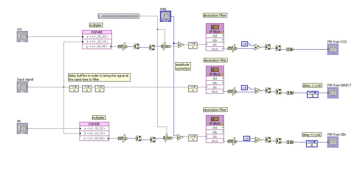
Figure 6 - Expander operation.
Figure 7 - Polyphase filter implementation in Labview FPGA.
Figure 8 - Expander implementation in LabView. The polyphase filters are the blue and green blocks.
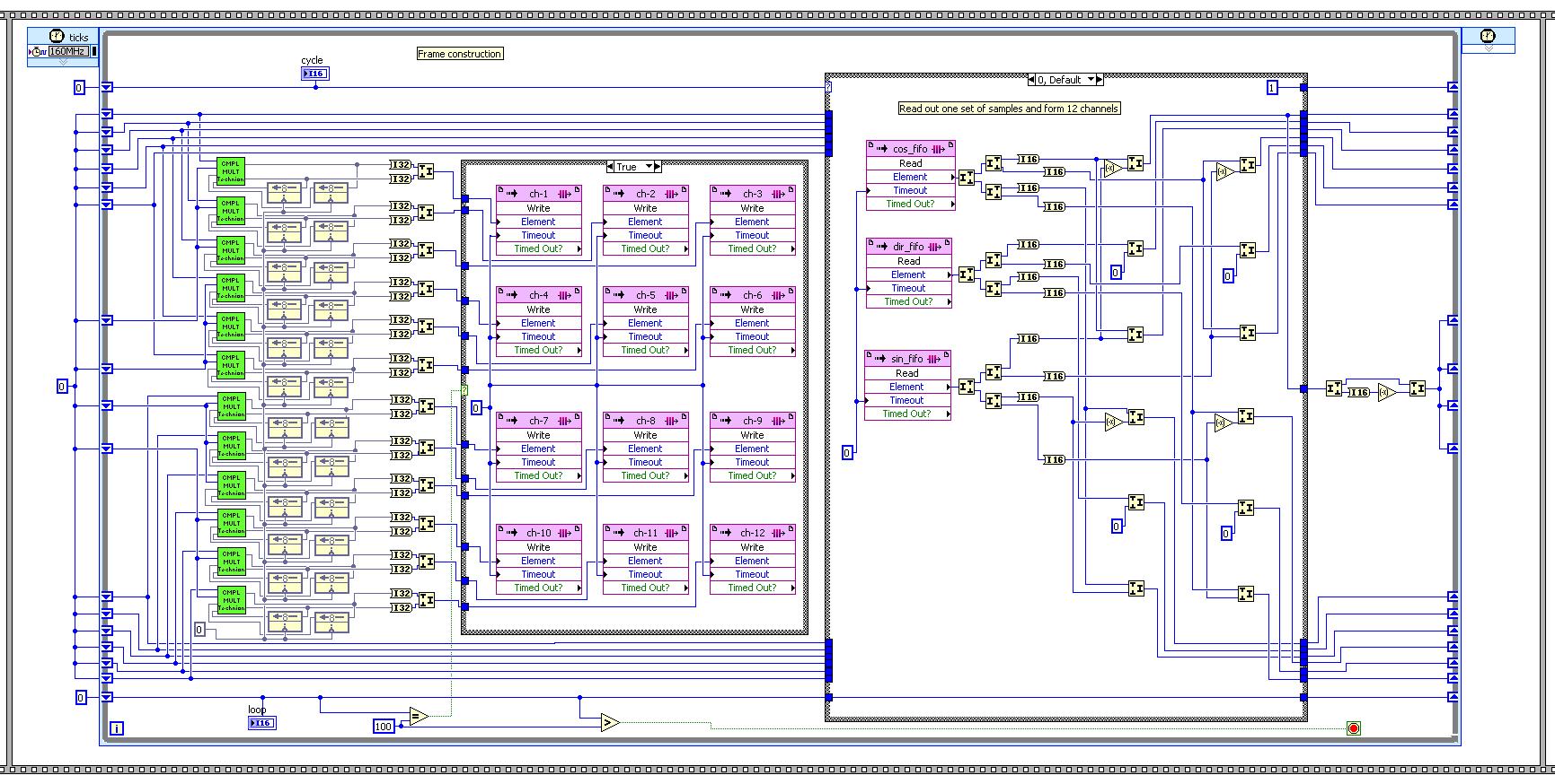
The samples the 2nd FPGA receives from the expander unit are routed in parallel to frame construction and sent via LVDS to the 3rd FPGA.
The frame construction obtains the Q matrix needed by the OMP algorithm used in the CTF to calculate the support and inverse of the reduced A matrix. The CTF block checks which frequency slices have energy and which slices do not have energy. In this way we can take out columns from the A matrix representing frequency slices without energy.
Figure 9 - Calculating the Q matrix.
The Q mat calculation uses 12 complex multipliers. In each cycle one set of samples is taken from the received data and sent to the Q matrix calculation for refining the matrix.
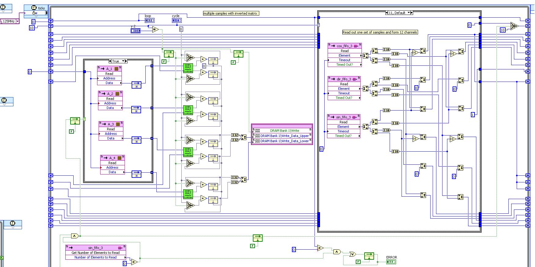
The 3rd FPGA contains the DSP unit. The DSP unit gets data from the 12 sampled channels created in the expander through the LVDS connection with the 2nd FPGA. The data is temporarily stored in on card memory. It then uses the inverted A matrix, calculated in the controller, and data taken from memory to reconstruct the slices of the original input. The reconstructed slices are moved to the controller processor using a DMA channel. Finally, the controller processor performs an FFT on those data received from the 3rd FPGA and displays the so found power spectrum.
Figure 10 - Calculating the slices.
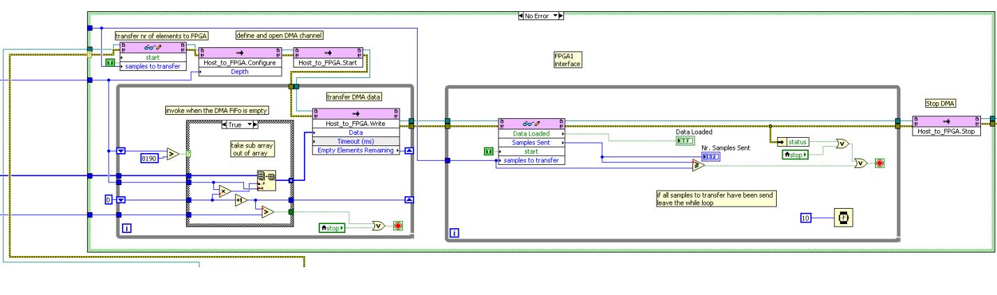
Operation of all FPGA's is controlled from the host machine, an NI chassis controller. The controller controls the dataflow in the algorithm and gives the trigger signals for each part to start working.
Figure 11 - Host VI - 1st FPGA dataflow control.
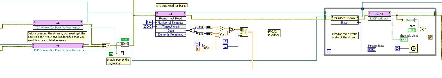
Figure 12 - Host VI - 2nd FPGA dataflow control.
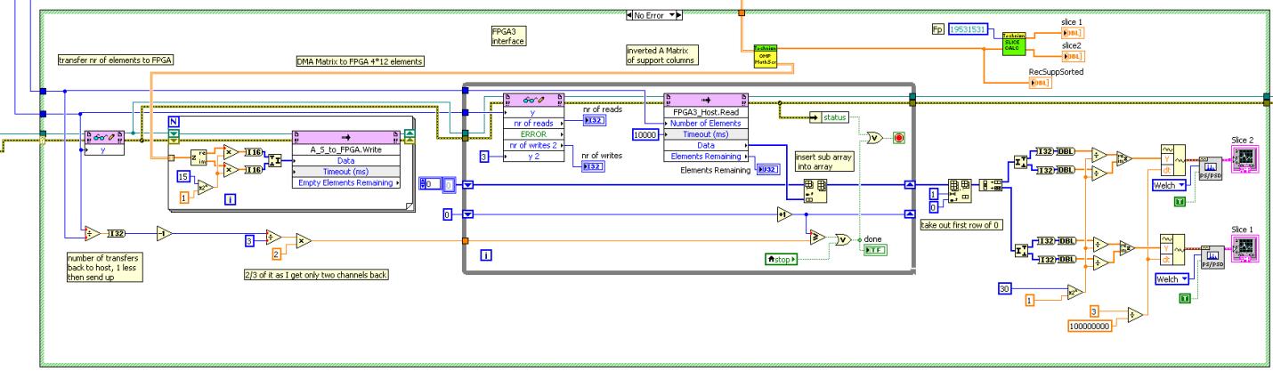
Figure 13 - Host VI - 3rd FPGA dataflow control.
The CTF is implemented on the controller as a math script VI. The CTF receives the full A matrix file and the Q matrix from the 2nd FPGA. Mathscript is similar to Matlab executing Matlab like code sequences on a NI machine. In the CTF, the order of the A matrix is reduced and thereafter inverted so we will only reconstruct those frequency slices with energy in them in the 3rd FPGA .
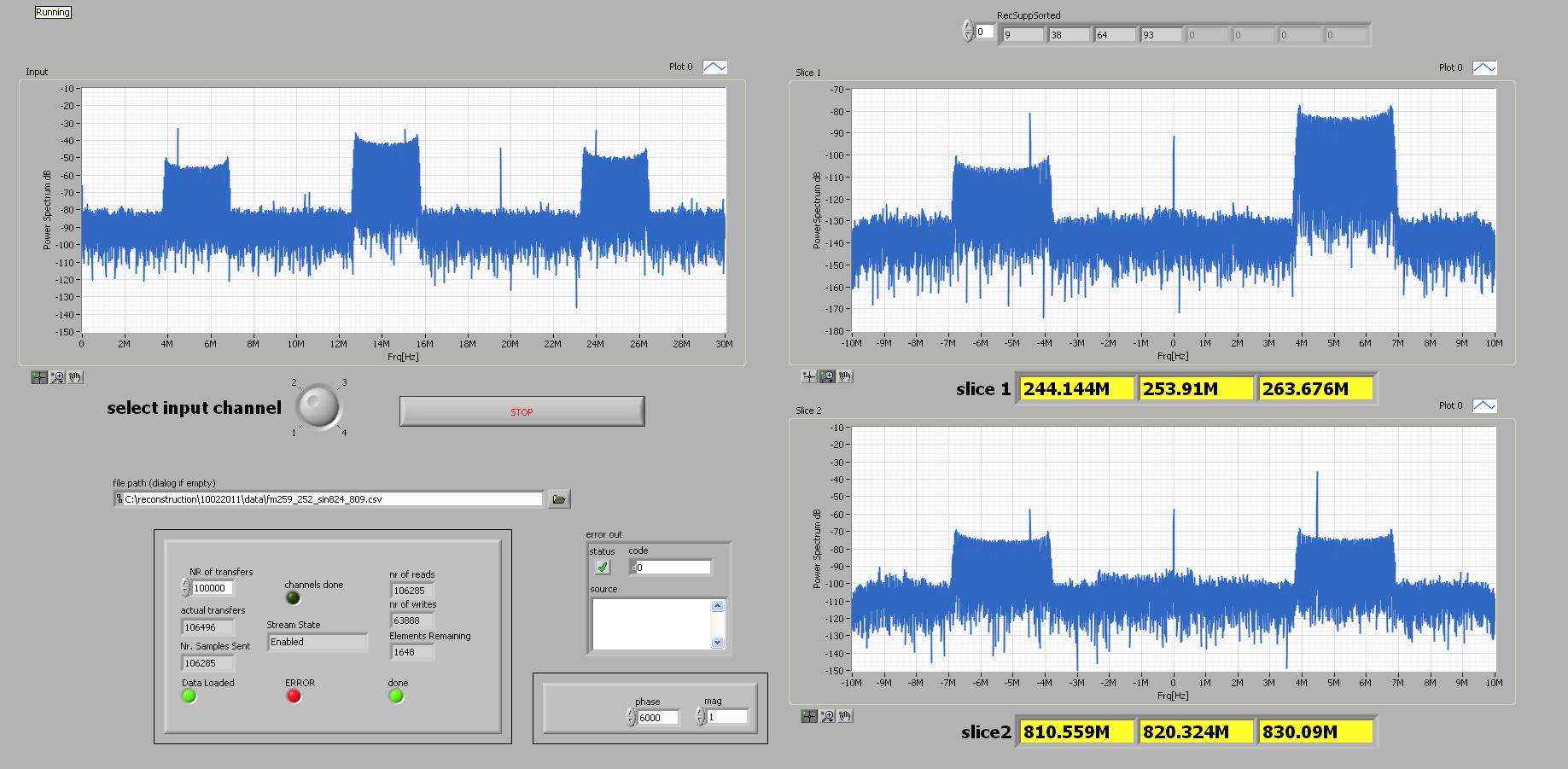
Figure 14 - The reconstruction front panel.
Figure 14 shows the reconstruction front panel. On the left hand side, we can see one of the input channels from the MWC. As we may notice, the signal shows aliased data which needs to be separated.
In the right hand side we can see figures representing two reconstructed slices. In this example the input was a FM signal at 252MHz and a sine wave at 824MHz. The algorithm reconstructed correctly the frequency slice of each of these signals and separated the signals such that they now can be fully reconstructed using a D/A. In the lower chart we can notice that the sine wave has more than 40 dB IMR (Image Rejection Ratio). Here we relate the FM as an image distortion converted by the mixers in the MWC. The same is seen in the upper chart where the FM signal has more than 40 dB IMR over the sine wave.
During the development of the system it was discovered that the algorithm features some phase sensitivity in the Expander block where the input signal is multiplied with a sine and a cosine function. Therefore, a phase controller was added to correct for phase shifts in the Expander. The phase shifts are caused by a lack of trigger capability between the MWC's periodic waveform and the A/D. Additionally some gain adjustment for the samples was added in order to improve reconstruction quality. The optimum gain is between 2 to 3.